
Free Lessons, Activities & More
Our lessons come with a collection of supplementary materials and useful links on the subject, as well as downloadable handouts, assessments, keys and much more.
All our teaching materials are downloadable entirely for free.
Subtypes:
Teaching Material
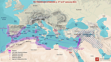
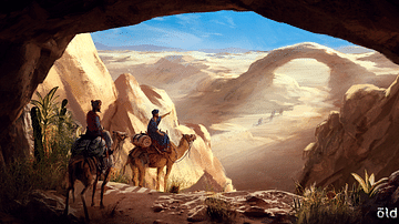
Phoenician Maritime Trade and Cultural Exchange
This lesson plan has two parts. During the first part, students...
Lesson Pack
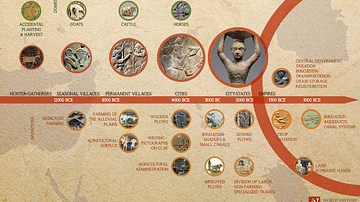
Mesopotamia: Innovations & Agriculture
This lesson pack on innovations and agriculture in ancient Mesopotamia...
Lesson Pack
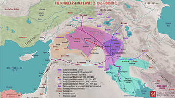
Mesopotamia: Empires & Warfare
This lesson pack on empires and warfare in ancient Mesopotamia...
Lesson Pack
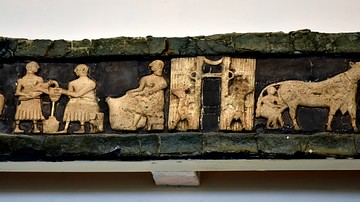
Mesopotamia: Daily Life
This lesson pack on daily life in ancient Mesopotamia includes...
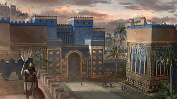
Lesson Pack
Mesopotamia: Government & Religion
This lesson pack on government and religion in ancient Mesopotamia...
Lesson Pack
Mesopotamia: Geography, Economy & Trade
This lesson pack on geography, economy and trade in ancient Mesopotamia...
Curated Collections
Collections are a great way to start finding supporting materials for your teaching. They are organized around different themes for which our editorial team selects the most appropriate content from our encyclopedia.
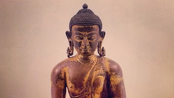
Collection
History of Buddhism
Buddhism was established in India by Siddhartha Gautama (the Buddha...

Image Gallery
Gallery of the Chateaux of the Loire Valley
This gallery gives an overview of 25 stunning châteaux in the Loire...

Collection
21 Famous Women of World History
This collection presents biographies of 21 famous women from world history...
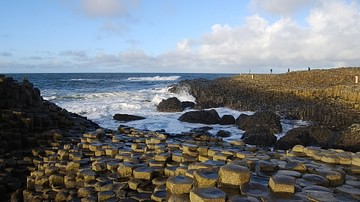
Image Gallery
Scenic Views of Ireland
According to one legend, Ireland takes its name from the Gaelic Eire...
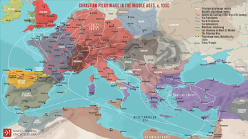
Image Gallery
10 Maps on European History
In this gallery of 10 maps on European history, we explore the dynamic...
Collection
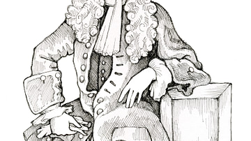
12 Key Enlightenment Philosophers
In this collection, we look at the lives, works, and ideas of the following...